- 您现在的位置:买卖IC网 > Sheet目录479 > MRF49XAT-I/ST (Microchip Technology)IC RF TXRX 433/868/915 16-TSSOP
MRF49XA
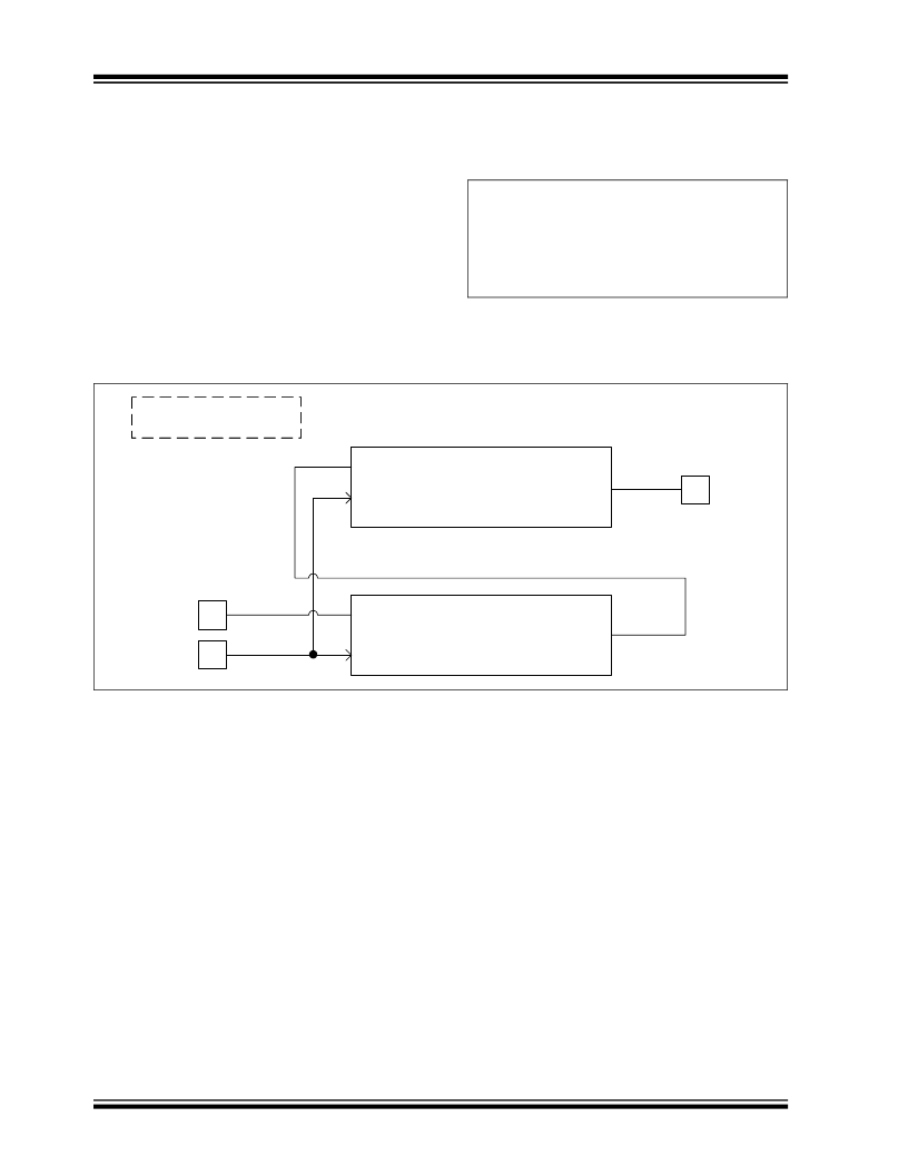
3.17 TX Register Buffered Data
Transmission
In Data Transmission mode (enabled by the TXDEN bit
(GENCREG<7>)), the TX data is clocked into one of
the two 8-bit data registers. The transmitter starts to
send the data from the first register (with the given bit
rate) when the TXCEN bit (PMCREG<5>) is set. The
initial value of the data registers (0xAA) can be used to
generate preamble. During this mode, the SDO pin is
monitored to check whether the register is ready (SDO
is high) to receive the next byte from the
microcontroller. The block diagrams of the Transmit
register, before and during transmit, are shown in
Figure 3-14 and Figure 3-15 , respectively.
The transmitter FSK modulation parameters are used
for calculating the resulting output frequency, as shown
in Equation 3-6 .
EQUATION 3-6:
f FSKOUT = f 0 + (-1)SIGN x (MB + 1) x (15 kHz)
where:
f 0 is the Channel Center Frequency
(see Register 2-6 for f 0 calculation)
MB is the 4-bit Binary Number (MODBW<3:0>)
SIGN = MODPLY XOR FSK
FIGURE 3-14:
TX REGISTER BLOCK DIAGRAM (BEFORE TRANSMIT)
TXCEN = 0
(Register Initial Fill-up)
SDI
8-Bit Shift Register
(Default: AAh)
SDO
TX_DATA
CLK
Serial Bus Data
SCLK
DS70590C-page 66
SDI
CLK
8-Bit Shift Register
(Default: AAh)
Preliminary
SDO
? 2009-2011 Microchip Technology Inc.
发布紧急采购,3分钟左右您将得到回复。
相关PDF资料
MRF89XA-I/MQ
TXRX ISM SUB-GHZ ULP 32QFN
MRF89XAM9A-I/RM
IC TXRX MOD 915MHZ ULP SUB-GHZ
MRX-001-433DR-B
MODULE RECEIVER 433MHZ 18DIP
MRX-002-433DR-B
MODULE RECEIVER 433MHZ 18DIP
MRX-002SL-433DR-B
MODULE RCVR 433MHZ SAW LN 24DIP
MRX-005-915DR-B
MODULE RECEIVER 915MHZ 18DIP
MRX-005SL-915DR-B
MODULE RCVR 915MHZ SAW LN 24DIP
MRX-007-433DR-B
MODULE RECEIVER 433MHZ 18DIP
相关代理商/技术参数
MRF49XAT-I/T
制造商:MICROCHIP 制造商全称:Microchip Technology 功能描述:ISM Band Sub-GHz RF Transceiver
MRF49XAT-I-ST
制造商:MICROCHIP 制造商全称:Microchip Technology 功能描述:ISM Band Sub-GHz RF Transceiver
MRF49XAT-I-T
制造商:MICROCHIP 制造商全称:Microchip Technology 功能描述:ISM Band Sub-GHz RF Transceiver
MRF4A(AMMO)
制造商:Bel Fuse 功能描述:FUSE
MRF5
制造商:Ferraz Shawmut 功能描述:
MRF50
制造商:Ferraz Shawmut 功能描述:
MRF500
制造商:Ferraz Shawmut 功能描述:
MRF5003
制造商:MOTOROLA 制造商全称:Motorola, Inc 功能描述:N-CHANNEL BROADBAND RF POWER FET
